


© CEA-Leti
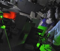
Helios silicon photonics
Defined as a Key Enabling Technology (KET) by the European Commission, ‘photonics, micro and nanoelectronics’ are set to receive €1.5bn of funding under Horizon 2020. One of the core aims of FP7’s replacement is to bring more new products to market and assist entrepreneurs with crossing ‘the valley of death’.
The Helios project, which received funding from the EU, was a large scale CMOS photonics project and ran from 2008 until 2012. The project focused on developing the microelectronics fabrication process for integrating photonics with CMOS circuits and to make the technology more widely available to a variety of users. Participants included key European CMOS photonics and electronics research centres, industrialists and potential users of the technology.
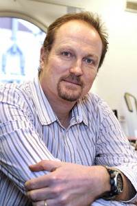
Speaking to Horizon2020projects.com, Laurent Fulbert, integrated photonics programme manager at CEA-Leti, outlined further information about Helios but began by outlining the current state of the industry.
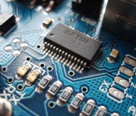
Silicon photonics is a way of integrating photonic functions together with electronics. The key idea is to use the same tools and manufacturing facilities as in microelectronics, known as ‘CMOS’ (Complementary metal-oxide-semiconductor), which has been shown that we can develop very complex circuits at very low cost.
When you want to make an optical link, you have to use different materials assembled together to make a complex module and this is very expensive. If you want to reduce costs and to reach high volume manufacturing, the only viable solution is to integrate all the functions of the silicon, so that’s why we use the ‘CMOS’ process.
The main drive for photonic innovation is data communications. Internet traffic is growing at a very fast rate and we need to transfer data at high speed, whether it’s over a long distance or between computers and data centres on a local network, or even between racks and between chips. Optics can do that more efficiently than electronics, so, by replacing a copper electrical line by optical fibres, you can reach higher speeds with lower power consumption, and therefore lower costs. There is a huge demand for photonic integrated circuits.
Helios
The Helios project was focused on silicon photonics and one of the objectives of the project were to build a complete photonic supply chain. We firstly developed all the technological processes to manufacture silicon photonic chips. The project was quite successful in developing the elementary building blocks – we have been able to demonstrate integrated silicon lasers and high speed modulators running at a rate of 40 Gb/s. We have developed the toolbox needed for making complex circuits.
There have been also some efforts on the design side. It is common in microelectronics to use Computer Aided Design tools and one of the objectives of Helios was to be able to design photonic circuits by using exactly the same design tools as in microelectronics, so there have been some efforts on building the design platform.
PLAT4M
We began a new project last year that follows up on Helios but with a different consortium and objectives. PLAT4M is an integrated project with a total EU funding worth €10.5m and 15 partners involved. The project is centred on manufacturing of photonics to help improve the maturity of the process and be ready for industrialisation.
In Helios, the majority of the efforts were devoted to development of the technology, the elementary building blocks. In PLAT4M, we are focusing on standardisation of the fabrication process with the ability to develop complex circuits with different building blocks to help provide a high yield and really improve maturity.
What are your thoughts on Horizon 2020 and do you believe it has a great enough focus on photonics investment?
The field of photonics may benefit from a public private partnership (PPP) under Horizon 2020. The KET is already set to receive additional funding compared to FP7 and with this PPP, total funding is expected to be €200m annually over the next seven years.
A positive step in Horizon 2020 is that it focuses greater efforts on development and innovation. FP7 really concentrated on R&D, whereas its replacement will centre its efforts on industrialisation and pilot lines, encouraging closer collaboration between businesses. I hope there will be a pilot line in silicon photonics to continue our progress under Helios and PLAT4M.
Do you think this new money will help the industry maintain its competitiveness in the photonics sector?
Definitely, yes. In the field of silicon photonics, there is strong competition with Asia and the USA – all the big players in microelectronics are interested in silicon photonics, for example Intel, IBM, HP and Samsung. These global corporations are working in silicon photonics, so it’s essential to maintain a good level of investment in Europe.
In Europe, we have also good industrial players that are entering the field of silicon photonics. In Helios, we involved end users, people that can use the technology to make products. In the PLAT4M project, we also have big microelectronic players like STMicroelectronics, which have decided to become heavily involved in silicon photonics; that is good news for Europe. We have been able to build a European-based supply chain for silicon photonics because we have the microelectronics family: designers, R&D institutes, e.g. CEA-Leti and IMEC, and academic labs. Europe has a range of end users of the technology, from the telecom sector to the sensing sector, from data communications to computing – they all rely on silicon photonics and the microelectronics.
Laurent Fulbert