


The EU next system in electronics
The ENIAC Joint Technology Initiative (JTI) was launched in 2008 and is a specialised public private partnership focusing on nanoelectronics. The key aims of the JTI include: ‘defining and implementing a nanoelectronic research agenda’; encouraging an increase in R&D investments; achieving synergy and co-ordination of European R&D efforts; and encouraging the participation of SMEs in R&D. The PPP brings together the European Commission with AENEAS, the European association representing the R&D actors in nanoelectronics. The JTI has helped implement recommendations regarding KETs in nanoelectronics and five pilot lines have been created, worth €730m.
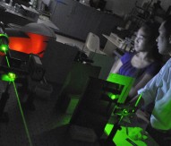
Taking place in Brussels at the European Parliament, and attended by Horizon 2020 Projects, a special press breakfast detailed the latest development of the JTIs. Speaking at the ‘Joint Technology Initiatives – Innovation in Action,’ Dr Andreas Wild, the executive director of ENIAC, drew attention to PPP’s developmental focus and the dramatic reduction in costings.
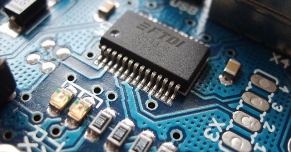
“This is an extremely capital intensive industry and therefore the high level of investments that are required depend to a large extent on the adequate availability of financial means. Maybe all of you have the closest point of contact with our products through in the smart card. Behind the gold pattern you see on the card, that is the chip; otherwise it is hidden and citizens do not see it displayed.
“No other industry has managed to do a cost reduction of a unit cost as our industry – one million times over 30 years. At the same time, energy cost-consumption has been reduced by 100,000 times – take the consumption of a car and think how essential you need to run it today. This is unique, but how is it achieved? This is achieved because the things that are realised and the active elements of a chip are getting smaller and smaller and therefore each one of them is costing less and less. However, to do that we need factories with extraordinary technical capabilities and the paradox is that the factory gets more and more expensive to produce objects that are less and less expensive. Now that indicates that we need to put forward sizable investments to have the technical capability to do inexpensively these smart devices. So our industry returns essentially upon the funding capabilities and upon the budgets that are available, both in the private sector and in the public sector.”
Wild continued by outlining the international expanse of the JTI in Europe as well as the significant participation of SMEs.
“Although we are behind, concentrated in a few locations in Europe, in our programme we have 22 country participants. If we sum up the contribution of the small countries, they exceed the contribution of the largest investor, France. Our project is also made up of 40% SMEs in the project. It is a technology that small and big, large and minute, research and industrial partners find their place. The whole eco-system is active. We are working with the Commission on how to implement these great ideas from the European Parliament and combine funding effectively to allow further development to continue.”
ECSEL
ENIAC and the related ARTEMIS JTI will be replaced by Electronic Components and System for European Leadership (ECSEL) JTI at the start of January 2014. ECSEL will aim to “keep Europe at the forefront of electronic components and systems and bridge faster the gap to exploitation,” according to a Commission Communication document. The PPP, through Horizon 2020, will receive around €1.215bn of funding, backed by a total of €3.6bn from industry partners and other sources; it will run for ten years.